
Collaboration among University of Iowa experts in electrical engineering, analytical computer modeling, and physics is advancing understanding of what is possible in the next generation of optoelectronic devices, such as high-performance computers, sensors, and photovoltaic cells.
Optoelectronic systems, in which photonic (light-based) and electronic materials work together, will be integral to the future of electronics, said Fatima Toor, an associate professor of electrical and computer engineering.
"This is because with the increasing miniaturization of electronics, we are reaching the limit on performance enhancements that can be achieved in traditional electronic devices such as computer processors," Toor said. "With the integration of photonics within conventional electronics, we can significantly enhance the performance of systems much beyond what is possible with electronics alone. This integration of photonic and electronic materials will benefit devices we use in our daily lives, such as a personal computers and LEDs as well as specialized systems such as medical devices or defense equipment."

Toor was a principal investigator of a recent grant with John P. Prineas, a professor of physics and astronomy.. Toor and Prineas developed nanowire semiconductors that enabled them to demonstrate two typically incompatible materials — silicon, an electronic material, and indium arsenide, a photonic material — could work together to build an optical system.
"The significance of combining these two materials is that (silicon) is the dominant electronic material today, with billions of dollars of commercialization infrastructure present globally, while (indium arsenide) is a photonic material and not as commercially mature,'" Toor said.
Nanowire semiconductors are currently inferior to conventional semiconductors, which are arranged in planar or layer format. This format inhibits growth of indium arsenide. Toor and Prineas were able to overcome this.
Their semiconductor nanowires created the possibility of structuring materials in all three dimensions, with a greater range of elements and compounds within the nanowire, and through ordered arrays and patterns of nanowires.
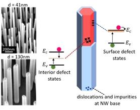
Results of the research detailing the viability of a new configuration of semiconductor nanowires was recently published in Optical Materials Express, a journal of The Optical Society. The paper stems from a $374,920 grant from the National Science Foundation.
"The research presented in the paper is on developing high quality optical structures that are at least 100 times thinner than a human hair," Toor said. "One cannot see these structures with a naked eye, they are that small. These high-quality optical nanostructures can be used in the computers you may use in 20 to 30 years from now."
Semiconductor heterostructures are used in the development of solid-state lighting, a modern lighting alternative to incandescent and fluorescent lighting now being used in commercial, residential, and street settings. The 2014 Nobel Prize in Physics was awarded to those behind the discoveries.
Toor is a University of Iowa Technology Institute faculty affiliate and director of the Toor Lab. Prineas directs the Prineas Research Group.
Toor’s team helped with the nanofabrication of templates on which the indium arsenide nanowires were grown using high vacuum molecular beam epitaxy, which is an area of expertise of Prineas. The team also characterized the optoelectronic properties of the nanowires using ultrafast spectroscopy systems available in the Prineas Lab.
“We plan to continue efforts in this area of combining so-called incompatible materials using nanowire structures to develop next generation optoelectronic devices,” Toor said. “The next steps would be to utilize more complex nanowire structures with, for example, quantum dots integrated in the nanowires, to enhance the utility of the III-V on Si systems.”